
 |
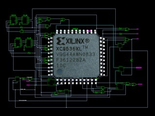
This project is a small board containing a CPLD and a SRAM IC. It has an SPI interface to utilize the SRAM. The CPLD is used to implement the SPI interface and address the SRAM. Only four pins are needed; this could be reduced to three if a bi-directional data line was used (like in I2C). It also has an auto-increment function. This means that the address only has to be written once in the initial three byte sequence that also contains the chip select and read/write selection. After these 3 bytes the data can be streamed in or out for any number of bytes. The CPLD is configured in a way that it does not need any external clock. The module could very easily be modified to address 4 (or even more) SRAM ICs with 512Kbytes each which would give 2Mbytes. The CPLD is programmed with the free XILINX ISE 10.1. |
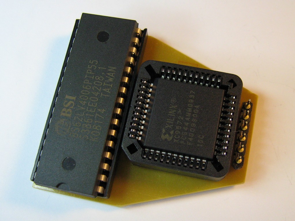
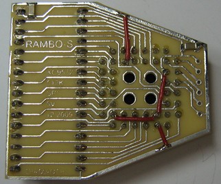
Here is a picture of the small module. The board could be much more compact if it was made in SMD technology but it is not possible to produce such tiny PCB layouts with my homebrew equipment. This one is quite compact too. The pins are the common SPI pins CS, CLK, MOSI and MISO and the 5V power supply. The system was tested with a clockrate up to 2.2MHz but higher rates may be possible.
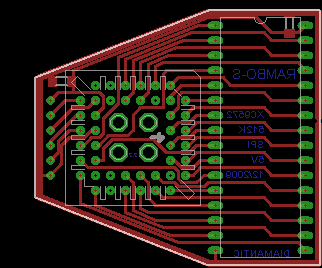
The PCB layout and the PCB.
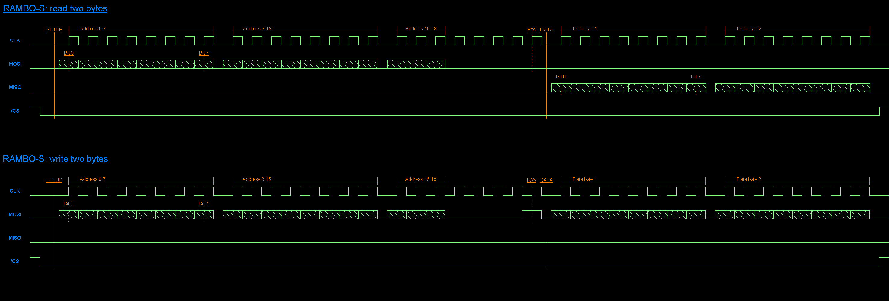
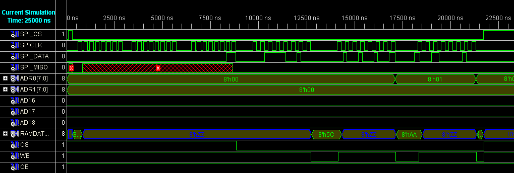
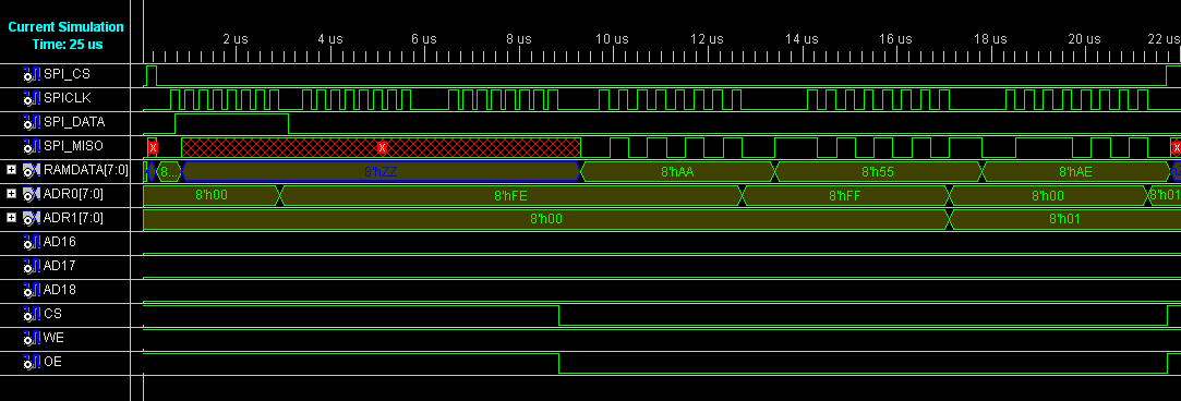
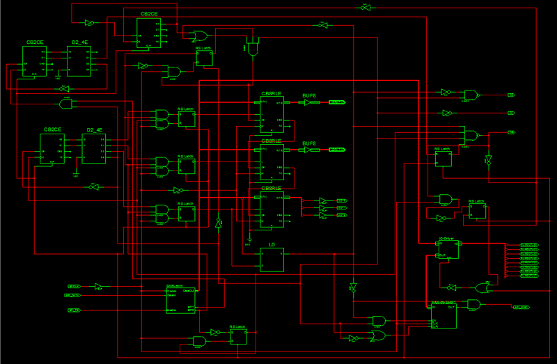
These are screenshots of the simulator diagram in XILINX ISE. The diagramm explains the funcionality. During the first three bytes the address is latched with the last falling clock. The address is incremented after each byte. When the counter overflows it jumps back to 0. The ISE project files are not freely available. This is because all other designs I have seen which have this functionallity use an external clock and cost money.
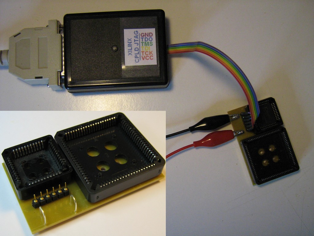
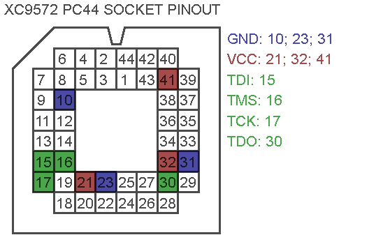
This is the setup for programming the device. I made a little adapter with JTAG interface for PC44 and PC84 devices. As the simulator and wave generator in the XILINX ISE is very accurate (see diagramm above) it is possible to do the entire debuging on the PC. The device only needs to be programmed once and with this little adapter the JTAG header can be spared in the end design.
|
LAST
|
NEXT
|